- Home
- Application
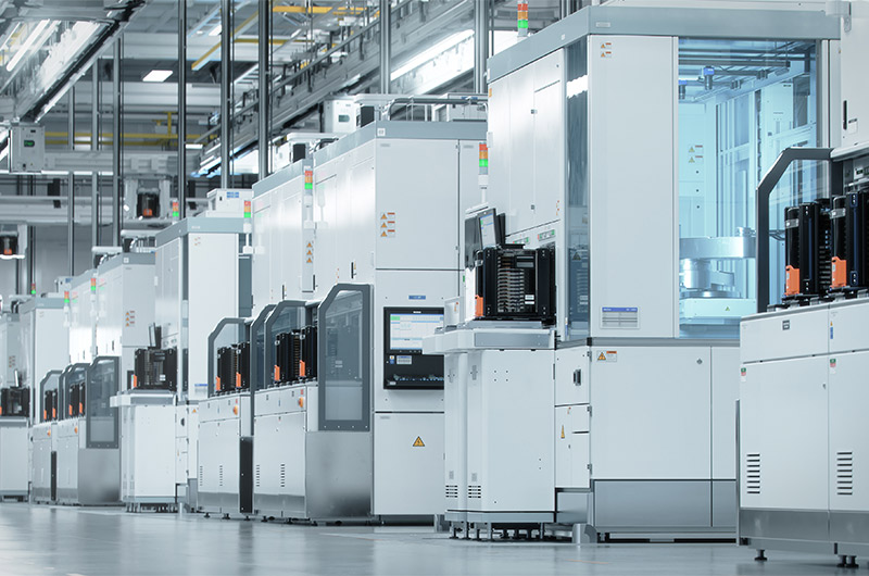
- Semiconductor
Semiconductor
Semiconductor Industry Application

Today, we can enjoy the convenience of life brought by many technologies every day, most of which are thanks to semiconductors. Semiconductor devices can be said to be the brains of modern technology applications. In addition to mobile phones and computers that everyone is familiar with, AI artificial intelligence, Internet of Things(IoT), 5G, etc. that have grown rapidly in recent years also require semiconductor materials as the core to make integrated circuits(IC).
What is Semiconductor?
A semiconductor is a material with special physical properties. At room temperature, it has an electrical conductivity value falling between that of a conductor and an insulator. Its conductivity can be changed by applying an external voltage. Semiconductors do not yet conduct electricity when no external voltage is applied; when a voltage is applied to the material, the originally nonconductive material becomes conductive, allowing current to flow.
High Purity and Pollution-Free Requirements
The semiconductor industry, which is so important and inseparable in our lives, contains many sophisticated integrated circuits and micro-electromechanical systems(MEMS) in the process, and in order to avoid the electrical properties of the product being affected, the manufacturing environment has strict requirements on cleanliness. Therefore, special attention should be paid to the process of conveying fluids to ensure that the manufacturing environment is maintained at a low pollution level so as not to affect the yield of products. If semiconductors are the core of advanced technology development, then pumps can be called the core of semiconductor manufacturing.

Process of Semiconductor
In the semiconductor wafer manufacturing process, some steps must rely on reliable chemical pumps to meet high-quality production requirements. The following briefly introduces the manufacturing process of wafers and chips.
Wafer Manufacturing Process:
Slicing
Crystal silicon ingot → Wafers → Lapping &Grinding → Cleaning → Etching → Polishing → Cleaning → Silicon Wafer
Chip Manufacturing Process:
Silicon Wafer → Film Deposition → Coated Photoresist → Expose → Developing → Etching → Ion implantation
Application of Sealless Magnetic Drive Pumps in Semiconductor Manufacturing Process
Wafer Surface Cleaning:
The reason why wafers need to be cleaned is to wash away impurities such as particles, chemical contaminants, and metal contaminants on the surface, so as to ensure the electrical parameters and characteristics of semiconductor components to achieve reliable quality. Chemicals such as hydrochloric acid, sulfuric acid, and hydrogen peroxide used in the cleaning process must maintain high purity, and these acid-base fluids are corrosive, so care must be taken to prevent leakage during transportation to avoid danger.
Developing, Etching:
In the wet process of wafers, as shown in the above steps, developers and chemical solutions are required for development and etching, etc. The cleanliness of these chemicals must be strictly controlled, as well as the corrosion and leakage problems during transportation must also be paid attention to.
Cleanroom:
Since today's wafers already have nano-level manufacturing technology, if particles or pollutants fall on the wafer surface, it may damage the entire wafer circuit. Therefore, in order to improve product quality and yield, it is necessary to strictly prevent dust particles enter the manufacturing environment. In the cleanroom equipment of the fab, pollution-free processing and reliability are the overall keys. For cleanliness requirements, certain types of clean room applications are suitable for sealless magnetic drive pumps, and PTFE and ETFE are best used to prevent chemicals and ultrapure water from leaking out of the pump and affecting the process.
Wastewater Treatment System:
While semiconductors are booming, in the component manufacturing process, in order to take into account the safety of operators and achieve environmental sustainability, the discharge and recycling of chemicals has also become a part of laws and regulations.
Chemicals used in general semiconductor manufacturing processes eventually become wastewater, such as organic, inorganic, heavy metal, and grinding wastewater, which must be mixed and separated before being recycled and reused. When building a complete recovery and discharge system, the internal pumps must also be strictly controlled. In this way, it can not only effectively prevent the pollution caused by the leakage of hazardous liquid chemicals, but also reduce operating costs and achieve the most ideal liquid waste recovery and disposal.
PTCXPUMP Sealless Magnetic Drive Pump Can Be Safely Applied To:
- Chemical Supply System
- Semiconductor Process: surface cleaning, developing, etching, etc.
- Wastewater Treatment System
PTCXPUMP sealless magnetic drive pump is used in the semiconductor industry to provide you with the best solution to transfer fluid. The design without mechanical seal, which is different from traditional mechanical seal pumps, can effectively avoid leakage, and the material is GFR-PP and CFR-ETFE, which has excellent corrosion resistance and is suitable for transporting highly corrosive liquid such as hydrochloric acid, sulfuric acid, hydrofluoric acid, and acetic acid or flammable and explosive fluids. In the semiconductor industry, it can be applied to various equipment systems.
In the PTCXPUMP sealless magnetic drive pump series, PTC-100 ~ PTC-251 are for small applications, and PTC-400 ~ PTC-675 are for medium and large applications. There are various models to meet your various operating needs. PTCXPUMP is committed to becoming your preferred choice for resting assured to use pumps.
Contact us and our professional team will work with you to select the best pump for your semiconductor application.